| CPC H01L 27/14614 (2013.01) [H01L 27/14621 (2013.01); H01L 27/14627 (2013.01); H01L 27/14636 (2013.01); H01L 27/1464 (2013.01); H01L 27/14645 (2013.01); H01L 27/14689 (2013.01); H01L 29/4236 (2013.01); H01L 29/42376 (2013.01)] | 20 Claims |

|
1. A device, comprising:
a semiconductor substrate;
a first source/drain region disposed within the semiconductor substrate;
a second source/drain region disposed within the semiconductor substrate and spaced apart from the first source/drain region in a first direction by a channel region of the semiconductor substrate;
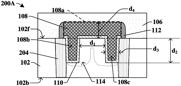
a horizontal gate electrode structure extending over a frontside of the semiconductor substrate, the horizontal gate electrode structure having a set of outer sidewalls separated from one another in a second direction perpendicular to the first direction;
a first vertical gate electrode structure extending downward from the horizontal gate electrode structure and into the semiconductor substrate, the first vertical gate electrode structure extending in the first direction along a first side of the channel region;
a second vertical gate electrode structure extending downward from the horizontal gate electrode structure and into the semiconductor substrate, wherein an inner sidewall of the second vertical gate electrode structure is spaced apart from an inner sidewall of the first vertical gate electrode structure, and the second vertical gate electrode structure extends in the first direction along a second side of the channel region;
a third vertical gate electrode structure extending from the frontside of the semiconductor substrate towards a backside of the semiconductor substrate, wherein a first side of the first vertical gate electrode structure is connected to a first side of the second vertical gate electrode structure by the third vertical gate electrode structure; and
wherein the set of outer sidewalls of the horizontal gate electrode structure extend outwardly in the second direction past outermost sidewalls of the first vertical gate electrode structure and the second vertical gate electrode structure.
|