| CPC H01L 27/0924 (2013.01) [H01L 21/02532 (2013.01); H01L 21/02579 (2013.01); H01L 21/0262 (2013.01); H01L 29/0673 (2013.01); H01L 29/0847 (2013.01); H01L 29/161 (2013.01); H01L 29/167 (2013.01); H01L 29/42392 (2013.01); H01L 29/66439 (2013.01); H01L 29/66795 (2013.01); H01L 29/775 (2013.01); H01L 29/7851 (2013.01)] | 20 Claims |

|
1. An integrated circuit device, comprising:
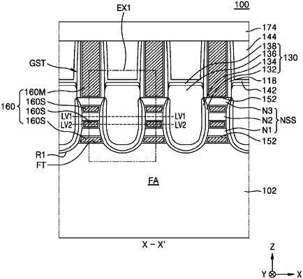
a fin-type active area along a first horizontal direction on a substrate;
a nanosheet stack including at least one nanosheet on a fin top of the fin-type active area, the at least one nanosheet being spaced apart from the fin top in a vertical direction;
a gate structure along a second horizontal direction crossing the first horizontal direction, the gate structure surrounding the at least one nanosheet; and
a source/drain area on the fin-type active area, the source/drain area contacting the at least one nanosheet, and the source/drain area including an outer blocking layer, an inner blocking layer, and a main body layer sequentially stacked on the fin-type active area,
wherein each of the outer blocking layer and the main body layer includes a Si1-xGex layer, where x≠0, and the inner blocking layer includes a Si layer, and
wherein a level of a lowermost surface of the source/drain area is lower than a level of the fin top in the vertical direction.
|