| CPC H01L 27/088 (2013.01) [H01L 29/4236 (2013.01); H01L 29/42364 (2013.01); H01L 29/6653 (2013.01); H01L 29/66621 (2013.01); H01L 29/7836 (2013.01)] | 20 Claims |

|
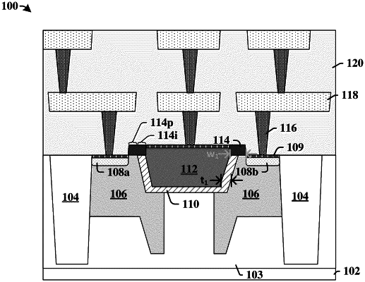
1. A method of forming a semiconductor device, comprising:
performing a first etching process by selectively exposing a substrate to a first etchant to produce a recess, wherein the recess is defined by sidewalls and a bottom surface, the bottom surface of the recess being below a topmost surface of the substrate;
doping the substrate to form a source extension region and a drain extension region respectively on opposite sides of the recess, wherein the source and drain extension regions extend from directly under the recess to the topmost surface of the substrate;
forming a gate dielectric layer over the sidewalls and the bottom surface of the recess;
forming a gate layer over the substrate, wherein a center portion of the gate layer is over the recess and in contact with the gate dielectric layer, the center portion of the gate layer surrounded by outer portions of the gate layer;
performing a second etching process on the gate layer to remove the outer portions of the gate layer by using a patterned hard mask over the center portion of the gate layer;
forming sidewall spacers along sidewalls of the gate layer and above the gate dielectric layer, wherein the sidewall spacers have a maximum width that is larger than a maximum thickness of the gate dielectric layer;
forming source/drain regions using the sidewall spacers as a mask, such that innermost edges of the source/drain regions are spaced apart from outermost edges of the gate dielectric layer, wherein the source/drain regions are respectively and directly on the source and drain extension regions; and
performing a planarization process such that top surfaces of the sidewall spacers and the gate layer are substantially planar;
wherein the gate layer is formed before the forming of the source/drain regions and after the doping to form the source extension region and the drain extension region, and wherein the source and drain extension regions are closer to a bottom surface of the substrate directly under the gate layer than directly under the source/drain regions.
|