| CPC H01L 27/0248 (2013.01) [G06F 30/392 (2020.01); H01L 21/82 (2013.01); H01L 27/0207 (2013.01); H01L 27/0928 (2013.01); H01L 21/823878 (2013.01)] | 19 Claims |

|
1. A method of forming an integrated circuit structure, the method comprising:
generating a tap cell layout pattern corresponding to fabricating a tap cell of an integrated circuit structure, the generating the tap cell layout pattern comprising:
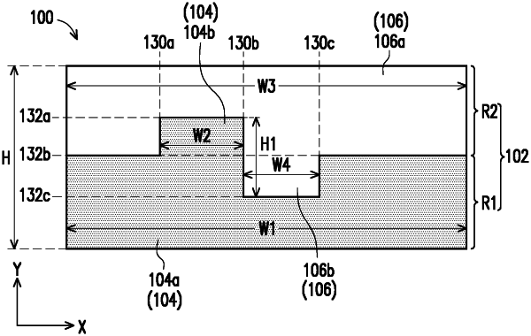
generating a first well layout pattern corresponding to fabricating a first well of the integrated circuit structure, the first well having a first dopant type;
generating a second well layout pattern corresponding to fabricating a second well of the integrated circuit structure, the second well having a second dopant type, wherein the first well layout pattern has a first jog pattern extending in the second well layout pattern and the second well layout pattern has a second jog pattern extending in the first well layout pattern; and
generating a first implant layout pattern at least overlapping the first jog pattern, the first implant layout pattern corresponding to fabricating a first set of implants of the integrated circuit structure, each implant of the first set of implants having the first dopant type, and at least one implant of the first set of implants being configured to be coupled to a first supply voltage;
generating a set of standard cell layout patterns adjacent to the tap cell layout pattern, the set of standard cell layout patterns corresponding to fabricating a set of standard cells of the integrated circuit structure; and
generating a set of active region layout patterns corresponding to fabricating a set of active regions of the integrated circuit structure, wherein the set of active region layout patterns comprises a first active region pattern continuously extending from the first jog pattern through the tap cell layout pattern and the standard cell layout pattern along the X direction.
|