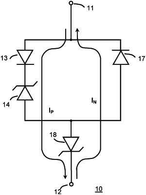
| CPC H01L 27/0248 (2013.01) [H01L 29/866 (2013.01)] | 20 Claims |

|
1. A semiconductor device, comprising:
a first terminal;
a second terminal;
a first P-N diode having an anode coupled to the first terminal and a cathode;
a first Zener diode in a series combination with the first P-N diode having a cathode coupled to the cathode of the first P-N diode and an anode;
a second P-N diode coupled in parallel with the series combination of the first P-N diode and the first Zener diode, the second P-N diode having a cathode coupled to the first terminal and an anode; and
a second Zener diode having a cathode coupled to the second terminal and an anode, the anode of the second Zener diode coupled to the anode of the second P-N diode and coupled to the anode of the first Zener diode;
wherein the semiconductor device comprises:
a semiconductor substrate of a first conductivity type having a first peak dopant concentration no less than approximately 1.0×10¹⁹ atoms/cm3;
a first semiconductor region of a second conductivity type opposite to the first conductivity type and having approximately the first peak dopant concentration, wherein:
the first semiconductor region forms a first P-N junction with the semiconductor substrate; and
the first P-N junction forms a junction of the first Zener diode;
a second semiconductor region of the second conductivity type on the first semiconductor region, wherein the second semiconductor region has a second peak dopant concentration that is less than the first peak dopant concentration;
a first doped region of the first conductivity type in the second semiconductor region and overlying the first semiconductor region;
a third semiconductor region laterally adjacent to the first semiconductor region and having the first conductivity type and a third peak dopant concentration;
a fourth semiconductor region of the first conductivity type on the third semiconductor region having a fourth peak dopant concentration that is less than the third peak dopant concentration;
a second doped region of the second conductivity type in the fourth semiconductor region and overlying the third semiconductor region; and
a third doped region of the second conductivity type contiguous with a bottom side of the semiconductor substrate and the second terminal, wherein the third doped region comprises approximately the first peak dopant concentration to provide a second P-N junction with the semiconductor substrate, and wherein the second P-N junction forms a junction of the second Zener diode.
|