| CPC H01L 25/0657 (2013.01) [H01L 21/565 (2013.01); H01L 23/3128 (2013.01); H01L 23/3135 (2013.01); H01L 24/48 (2013.01); H01L 25/50 (2013.01); H01L 24/32 (2013.01); H01L 24/33 (2013.01); H01L 24/73 (2013.01); H01L 2224/32145 (2013.01); H01L 2224/32225 (2013.01); H01L 2224/33181 (2013.01); H01L 2224/48091 (2013.01); H01L 2224/48106 (2013.01); H01L 2224/48145 (2013.01); H01L 2224/48227 (2013.01); H01L 2224/73215 (2013.01); H01L 2224/73265 (2013.01); H01L 2225/06506 (2013.01); H01L 2225/0651 (2013.01); H01L 2225/06562 (2013.01); H01L 2225/06586 (2013.01)] | 21 Claims |
|
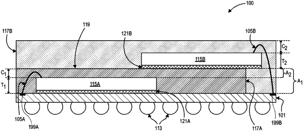
1. A semiconductor package, comprising:
a substrate, the substrate having a first outermost sidewall laterally opposite a second outermost sidewall;
a first die on the substrate, the first die electrically coupled to the substrate, and the first die having a first sidewall laterally opposite a second sidewall;
a first molding compound encapsulating the first die on the substrate, the first molding compound in contact with the first sidewall and the second sidewall of the first die, and the first molding compound having a first outermost sidewall and a second outermost sidewall, the second outermost sidewall laterally opposite the first outermost sidewall, and the first outermost sidewall of the first molding compound in vertical alignment with the first outermost sidewall of the substrate;
a second die on the first molding compound, the second die having a portion electrically coupled to the substrate, the portion of the second die extending laterally beyond the second outermost sidewall of the first molding compound; and
a second molding compound encapsulating the second die and at least one portion of the first molding compound.
|