| CPC H01L 23/66 (2013.01) [H01L 21/76825 (2013.01); H01L 21/76832 (2013.01); H01L 21/76834 (2013.01); H01L 21/76879 (2013.01); H01L 23/5283 (2013.01); H01L 23/53233 (2013.01); H01L 23/53238 (2013.01); H01L 2223/6605 (2013.01)] | 16 Claims |
|
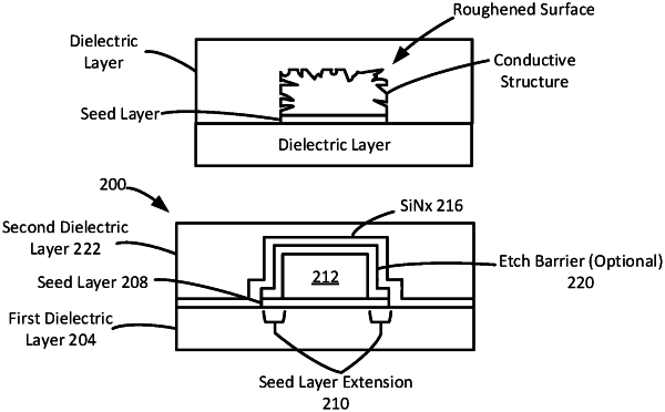
1. An integrated circuit package comprising:
a first layer comprising a dielectric material;
a structure comprising a conductive material over the first layer, wherein the structure comprises a surface roughness of 50 nm or less;
a second layer over the structure, the second layer compositionally distinct from the first layer, wherein the second layer is a single layer conformal with the structure, and wherein the second layer has an uppermost surface above an uppermost surface of the structure;
a third layer over the first layer, the structure, and the second layer, the third layer comprising the dielectric material and compositionally distinct from the second layer;
wherein the structure includes a first portion having a first width and a second portion having a second width that is wider than the first width;
wherein the second portion extends laterally beyond a first side of the first portion by 1 μm to 5 μm, and wherein the second portion extends laterally beyond a second side of the first portion by 1 μm to 5 μm; and
wherein the second layer comprises silicon and one or more of nitrogen, carbon, and oxygen.
|