| CPC H01L 23/5389 (2013.01) [H01L 21/4857 (2013.01); H01L 21/568 (2013.01); H01L 23/3128 (2013.01); H01L 25/18 (2013.01); H01L 25/50 (2013.01)] | 20 Claims |

|
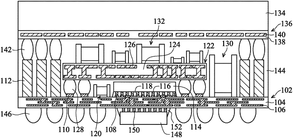
1. A method for forming a package structure, comprising:
forming first conductive structures and a first semiconductor die on a same side of a redistribution structure;
forming an interposer substrate over the redistribution structure, wherein the first semiconductor die is between the interposer substrate and the redistribution structure, and edges of the interposer substrate extend beyond edges of the first semiconductor die;
forming a second semiconductor die on the redistribution structure, wherein the first semiconductor die and the second semiconductor die are disposed on opposite sides of the redistribution structure;
forming an interconnection structure over the interposer substrate;
forming a protective layer to be in contact with the interconnection structure, the interposer substrate, and the redistribution structure;
wherein the first semiconductor die, and the protective layer are separated from the second semiconductor die, and the protective layer extends between the first semiconductor die and the interposer substrate.
|
|
8. A method for forming a package structure, comprising:
forming first conductive structures and a first semiconductor die on a first side of a redistribution structure, wherein the first conductive structures are higher than the first semiconductor die;
forming second conductive structures on the first semiconductor die;
forming an interposer substrate in contact with the first conductive structures, wherein the interposer substrate has a greater width than the first semiconductor die;
forming a second semiconductor die on a second side of the redistribution structure;
forming a first passive device element on the first side of the redistribution structure, wherein the first passive device element and the first semiconductor die have different heights;
forming a protective layer in contact with the first conductive structures and the second conductive structures;
forming third conductive structures on the first semiconductor die and separated from the protective layer; and
forming a first underfill material between the first semiconductor die and the redistribution structure and surrounding the third conductive structures, wherein the protective layer and the third conductive structures are separated by the first underfill material.
|
|
14. A method for forming a package structure, comprising:
forming first conductive structures and a first semiconductor die on a first side of a redistribution structure;
forming second conductive structures on the first semiconductor die;
forming an interposer substrate, wherein a first side of the interposer substrate is in contact with the first conductive structures, and the interposer substrate has a greater width than the first semiconductor die;
forming a second semiconductor die on a second side of the interposer substrate, wherein widths of the first semiconductor die and the second semiconductor die are different;
forming a first passive device element on the first side of the redistribution structure, wherein the first passive device element and the first semiconductor die have different heights; and
forming a protective layer between the first passive device element and the interposer substrate, and in contact with sidewalls of the interposer substrate, wherein the protective layer is in contact with the first semiconductor die, and is separated from the second semiconductor die by the redistribution structure.
|