| CPC H01L 23/5286 (2013.01) [H01L 21/823475 (2013.01); H01L 29/0696 (2013.01)] | 20 Claims |

|
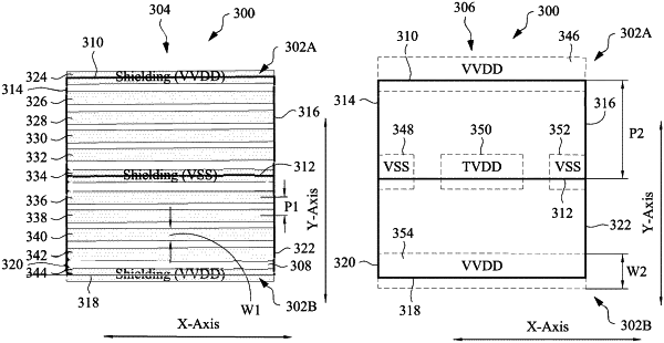
1. A semiconductor device, comprising:
a semiconductor substrate including one or more active semiconductor components wherein a front side is defined over the semiconductor substrate and a back side is defined beneath the semiconductor substrate;
a first front side power rail in a first front side metal layer at the front side of the semiconductor substrate, the first front side power rail being configured to receive a first reference power voltage; and
a first back side power rail, a second back side power rail, a third back side power rail and a fourth back side power rail in a first back side metal layer at the back side of the semiconductor substrate and each extending in a first direction;
the first back side power rail being configured to receive a second reference power voltage;
the second back side power rail being configured to receive a third reference power voltage;
each of the third and fourth back side power rails being configured to receive the first reference power voltage;
within a span of a first cell that is defined relative to the first direction,
the second back side power rail being between the third and the fourth back side power rails relative to the first direction;
relative to a second direction that is substantially perpendicular to the first direction, the first front side power rail at least partially overlapping the third back side power rail and the fourth back side power rail; and
the first reference power voltage, the second reference power voltage, and the third reference power voltage being different from each other.
|