| CPC H01L 23/5283 (2013.01) [H01L 21/02063 (2013.01); H01L 21/32125 (2013.01); H01L 21/67207 (2013.01); H01L 21/76814 (2013.01); H01L 21/76816 (2013.01); H01L 21/76831 (2013.01); H01L 21/7684 (2013.01); H01L 21/76843 (2013.01); H01L 21/76871 (2013.01); H01L 21/76879 (2013.01); H01L 21/76882 (2013.01); H01L 23/5226 (2013.01); H01L 23/53209 (2013.01); H01L 23/53223 (2013.01); H01L 23/53233 (2013.01); H01L 23/53238 (2013.01); H01L 23/53252 (2013.01); H01L 23/53266 (2013.01)] | 20 Claims |
|
1. An integrated tool for performing semiconductor processing, the integrated tool, comprising:
a set of process chambers of the integrated tool that are interconnected under vacuum and configured to perform a set of processes of a method for creating a dual metal interconnect, the method including:
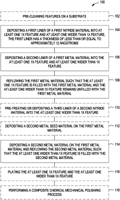
depositing a first liner of a first nitride material into at least one 1X feature and at least one wider than 1X feature, the first liner has a thickness of less than or equal to approximately 12 angstroms, wherein X is a minimum feature width;
depositing a second liner of a first metal material into the at least one 1X feature and at least one wider than 1X feature;
reflowing the first metal material such that the at least one 1X feature is filled with the first metal material and the at least one wider than 1X feature remains partially filled;
depositing a second metal material on the first metal material; and
reflowing the second metal material such that the at least one wider than 1X feature is filled with the second metal material.
|