| CPC H01L 23/528 (2013.01) [H01L 21/02433 (2013.01); H01L 21/2011 (2013.01); H01S 5/0213 (2013.01)] | 19 Claims |

|
1. A semiconductor device, comprising:
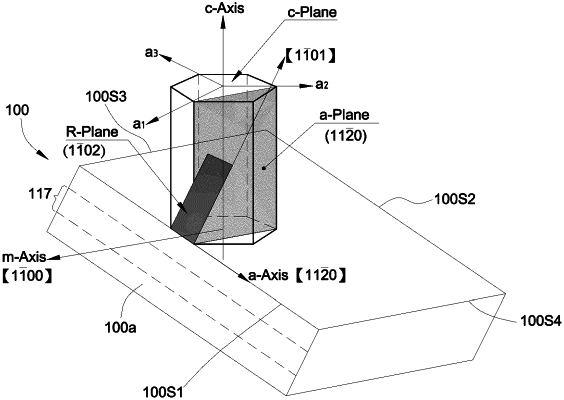
a substrate, comprising an upper surface, a first side surface, a second side surface opposite to the first side surface, a third side surface connecting the first side surface and the second side surface, and a fourth side surface opposite to the third side surface;
wherein the upper surface comprises a first edge connecting the first side surface, a second edge opposite to the first edge and connecting the second side surface, a third edge connecting the third side surface, and a fourth edge opposite to the third edge and connecting the fourth side surface;
a horizontal direction parallel to the upper surface and a vertical direction perpendicular to the upper surface;
a first modified trace formed on the first side surface;
and
a semiconductor stack formed on the upper surface, comprising a lower surface connecting the upper surface of the substrate, and the lower surface comprises a fifth edge adjacent to the first edge and a sixth edge opposite to the fifth edge and adjacent to the second edge;
wherein a shortest distance between the first edge and the fifth edge is S1 μm, and a shortest distance between the second edge and the sixth edge is S2 μm;
wherein in a lateral view viewing from the third side surface, the first side surface forms a first acute angle with a degree of θ1 with the vertical direction, the second side surface forms a second acute angle with a degree of θ2 with the vertical direction, and a distance between the first modified trace and the upper surface in the vertical direction is D1 μm; and
wherein S1, S2, θ1, θ2 and D1 satisfy the equation:
D1≤0.2×(S1+S2)/tan θa, wherein θa=(θ1+θ2)/2.
|