| CPC H01L 23/5226 (2013.01) [H01L 21/76802 (2013.01); H01L 21/76828 (2013.01); H01L 21/76832 (2013.01); H01L 21/76834 (2013.01); H01L 21/76843 (2013.01); H01L 21/76877 (2013.01); H01L 23/53214 (2013.01); H01L 23/53228 (2013.01); H01L 23/53266 (2013.01)] | 20 Claims |

|
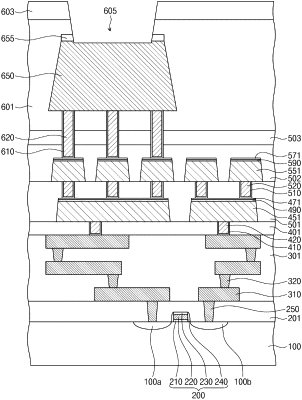
17. A semiconductor device comprising:
a substrate;
a first metal pattern on the substrate;
a second metal pattern on the first metal pattern;
a metal oxide pattern on the second metal pattern;
an antireflective pattern on the metal oxide pattern; and
a third metal pattern on the antireflective pattern,
wherein the first metal pattern includes copper (Cu),
each of the second metal pattern and the third metal pattern includes aluminum (Al),
the metal oxide pattern includes titanium oxide (TiO2),
the antireflective pattern includes titanium nitride (TiN), and
a thickness of the third metal pattern in a direction that is perpendicular to a top surface of the substrate is greater than a thickness of the second metal pattern in the direction.
|