| CPC H01L 23/5226 (2013.01) [H01L 21/4857 (2013.01); H01L 23/3121 (2013.01); H01L 23/3128 (2013.01); H01L 23/3192 (2013.01); H01L 23/5389 (2013.01); H01L 24/08 (2013.01); H01L 24/94 (2013.01); H01L 23/49816 (2013.01); H01L 23/562 (2013.01); H01L 2224/0801 (2013.01); H01L 2224/08112 (2013.01)] | 20 Claims |

|
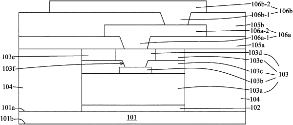
1. A semiconductor structure, comprising:
a die;
a molding surrounding the die;
a first dielectric layer disposed over the die and the molding;
a second dielectric layer disposed between the first dielectric layer and the die, and between the first dielectric layer and the molding; and
a conductive trace, wherein the conductive trace comprises:
a via portion disposed in the second dielectric layer; and
a land portion disposed in the first dielectric layer, wherein the land portion is electrically connected to the die,
wherein a material content ratio in the first dielectric layer is substantially greater than that in the second dielectric layer, and the material content ratio substantially inversely affects a mechanical strength of the first dielectric layer and the second dielectric layer.
|