US 11,948,880 B2
SOI substrate and related methods
Mark Griswold, Gilbert, AZ (US); and Michael J. Seddon, Gilbert, AZ (US)
Assigned to SEMICONDUCTOR COMPONENTS INDUSTRIES, LLC, Scottsdale, AZ (US)
Filed by SEMICONDUCTOR COMPONENTS INDUSTRIES, LLC, Phoenix, AZ (US)
Filed on Oct. 4, 2022, as Appl. No. 17/937,918.
Application 16/929,378 is a division of application No. 15/961,642, filed on Apr. 24, 2018, granted, now 10,741,487, issued on Aug. 11, 2020.
Application 17/937,918 is a continuation of application No. 16/929,378, filed on Jul. 15, 2020, granted, now 11,495,529.
Prior Publication US 2023/0025410 A1, Jan. 26, 2023
This patent is subject to a terminal disclaimer.
Int. Cl. H01L 21/78 (2006.01); H01L 21/02 (2006.01); H01L 21/786 (2006.01); H01L 23/12 (2006.01); H01L 23/34 (2006.01); H01L 23/522 (2006.01)
CPC H01L 23/5222 (2013.01) [H01L 21/0226 (2013.01); H01L 21/786 (2013.01); H01L 23/12 (2013.01); H01L 23/34 (2013.01)] 20 Claims
OG exemplary drawing
 
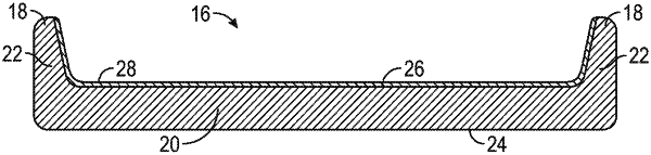
1. A silicon-on-insulator (SOI) die comprising:
a silicon layer comprising a first side and a second side;
an insulative layer coupled directly to the second side of the silicon layer,
wherein the insulative layer is coupled to silicon only through the second side of the silicon layer;
wherein the SOI die is singulated;
wherein the insulative layer comprises an insulative material that fills an entire area within an outer perimeter of the insulative layer; and
wherein the silicon layer is thinned through a backgrinding process.