| CPC H01L 23/49589 (2013.01) [H01L 23/4951 (2013.01); H01L 23/49524 (2013.01); H01L 24/32 (2013.01); H01L 24/73 (2013.01); H01L 24/11 (2013.01); H01L 24/13 (2013.01); H01L 24/16 (2013.01); H01L 24/92 (2013.01); H01L 2224/11462 (2013.01); H01L 2224/13147 (2013.01); H01L 2224/13564 (2013.01); H01L 2224/1357 (2013.01); H01L 2224/16245 (2013.01); H01L 2224/32265 (2013.01); H01L 2224/73203 (2013.01); H01L 2224/73253 (2013.01); H01L 2224/9211 (2013.01); H01L 2924/19015 (2013.01); H01L 2924/19041 (2013.01); H01L 2924/19103 (2013.01); H01L 2924/19104 (2013.01)] | 20 Claims |

|
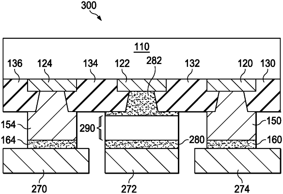
1. An integrated circuit (IC) comprising:
a silicon wafer;
a first conductive line having first and second surfaces, wherein the second surface is opposite the first surface, and the first surface of the first conductive line is coupled to the silicon wafer;
a second conductive line having first and second surfaces, wherein the second surface is opposite the first surface, and the first surface of the second conductive line is coupled to the silicon wafer;
a first insulation block having first and second portions, wherein:
the first portion has first and second surfaces, the first surface of the first portion is opposite the second portion of the first surface, and the first surface of the first portion is coupled to the silicon wafer; and
the second portion has first and second surfaces, the first surface of the second portion is opposite the second portion of the second surface, the second portion of the second surface is a continuation of the second surface of the first portion, and the first surface of the second portion is coupled to the second surface of the first conductive line;
a second insulation block laterally spaced from the first insulation block and having third, fourth and fifth portions, wherein:
the third portion has first and second surfaces, the first surface of the third portion is opposite the second surface of the third portion, the first surface of the third portion is coupled to the second surface of the first conductive line;
the fourth portion has first and second surfaces, the first surface of the fourth portion is opposite the second surface of the fourth portion, the second surface of the fourth portion is a continuation of the second surface of the third portion, the first surface of the fourth portion is coupled to the silicon wafer; and
the fifth portion has first and second surfaces, the first surface of the fifth portion is opposite the second surface of the fifth portion, the first surface of the fifth portion is coupled to the second surface of the second conductive line, and the second surface of the fifth portion is a continuation of the second surface of the fourth portion;
a third insulation block laterally spaced from the second insulation block and having sixth, seventh and eighth portions, wherein:
the sixth portion has first and second surfaces, the first surface of the sixth portion is opposite the second surface of the sixth portion, and the first surface of the sixth portion is coupled to the second surface of the second conductive line; and
the seventh portion has first and second surfaces, the first surface of the seventh portion is opposite the second surface of the seventh portion, the second surface of the seventh portion is a continuation of the second surface of the sixth portion, and the first surface of the seventh portion is coupled to the silicon wafer;
a conductive pillar coupled to the second surface of the first conductive line, the second portion, and the third portion, and extending beyond the first and second insulation blocks; and
a conductive adhesive block coupled to the second surface of the second conductive line, the fifth portion and the sixth portion.
|