| CPC H01L 23/481 (2013.01) [H01L 21/4846 (2013.01); H01L 21/76898 (2013.01); H01L 23/13 (2013.01); H01L 23/5385 (2013.01); H01L 23/5389 (2013.01); H01L 24/19 (2013.01); H01L 24/20 (2013.01); H01L 24/97 (2013.01); H10N 10/01 (2023.02); H01L 21/561 (2013.01); H01L 21/568 (2013.01); H01L 23/49811 (2013.01); H01L 24/16 (2013.01); H01L 24/32 (2013.01); H01L 24/48 (2013.01); H01L 24/73 (2013.01); H01L 24/83 (2013.01); H01L 24/92 (2013.01); H01L 2224/0401 (2013.01); H01L 2224/04042 (2013.01); H01L 2224/04105 (2013.01); H01L 2224/12105 (2013.01); H01L 2224/16227 (2013.01); H01L 2224/32225 (2013.01); H01L 2224/48091 (2013.01); H01L 2224/48227 (2013.01); H01L 2224/73267 (2013.01); H01L 2224/83005 (2013.01); H01L 2224/83191 (2013.01); H01L 2224/83192 (2013.01); H01L 2224/92244 (2013.01); H01L 2224/97 (2013.01); H01L 2924/00014 (2013.01); H01L 2924/14 (2013.01); H01L 2924/1421 (2013.01); H01L 2924/1431 (2013.01); H01L 2924/1434 (2013.01); H01L 2924/1436 (2013.01); H01L 2924/1437 (2013.01); H01L 2924/1461 (2013.01)] | 20 Claims |

|
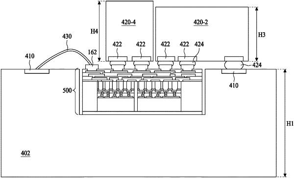
1. A structure comprising:
a first package within a recess in a first substrate, the first package comprising:
a first die encapsulated with an encapsulant; and
a first redistribution structure over the first die and the encapsulant, the first redistribution structure being electrically coupled to the first die, the first die being between the first redistribution structure and a bottom surface of the recess in the first substrate;
a first sensor bonded to the first package and the first substrate by a first set of solder connectors, the first sensor spans across a gap between a sidewall of the recess of the first substrate and an exterior sidewall of the first package; and
a second sensor bonded to the first package by a second set of solder connectors.
|