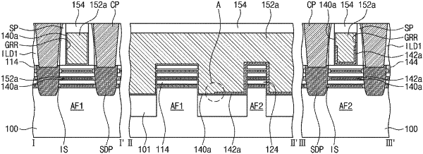
| CPC H01L 21/823821 (2013.01) [H01L 21/0332 (2013.01); H01L 21/0337 (2013.01); H01L 21/3086 (2013.01); H01L 27/0922 (2013.01); H01L 29/0642 (2013.01); H01L 29/66545 (2013.01); H01L 29/66553 (2013.01); H01L 29/6681 (2013.01); H01L 29/7851 (2013.01)] | 20 Claims |

|
1. A semiconductor device, comprising:
a device isolation layer between a first active region and a second active region of a substrate;
a first active fin on the first active region;
a second active fin on the second active region;
a first electrode pattern on the first active fin and the second active fin; and
a second electrode pattern between the first electrode pattern and the second active fin,
wherein the second electrode pattern extends on the device isolation layer and has an end adjacent to the first active region of the substrate,
wherein a sidewall of the end of the second electrode pattern has an angle relative to a top surface of the substrate, and
wherein the angle relative to the top surface of the substrate ranges from 91° to 100°, a top surface of the second electrode pattern extends further in a direction away from the second active fin than a bottom surface of the second electrode pattern, and the end of the second electrode pattern adjacent to the first active region of the substrate has a continuous slope.
|