| CPC H01L 21/823481 (2013.01) [H01L 21/0332 (2013.01); H01L 21/0337 (2013.01); H01L 27/088 (2013.01)] | 20 Claims |

|
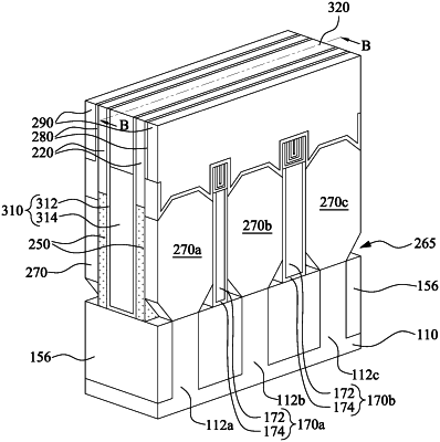
1. A method for forming a semiconductor device, comprising:
forming a pair of fin structures each having a stack of alternating first and second semiconductor layers over a substrate and a hard mask layer over the stack;
forming a dummy fin structure laterally between the pair of fin structures and having a top surface in a position lower than the hard mask layers of the stacks;
depositing a hafnium oxide layer over the dummy fin structure at a first temperature lower than a first crystallization temperature of the hafnium oxide layer;
depositing a silicon oxide layer over the hafnium oxide layer at a second temperature lower than the first crystallization temperature of the hafnium oxide layer;
performing a planarization process on the hafnium oxide layer and the silicon oxide layer to expose the hard mask layers of the stacks;
annealing the hafnium oxide layer at a third temperature higher than the first crystallization temperature of the hafnium oxide layer and lower than a second crystallization temperature of the silicon oxide layer;
after annealing the hafnium oxide layer, removing the hard mask layers of the stacks;
removing the first semiconductor layers of the stacks such that the second semiconductor layers of the stacks are suspended over the substrate; and
forming a gate structure to surround each of the suspended second semiconductor layers of the stacks.
|