| CPC H01L 21/823481 (2013.01) [H01L 21/762 (2013.01); H01L 21/76229 (2013.01); H01L 21/823431 (2013.01); H01L 27/0886 (2013.01); H01L 29/0649 (2013.01); H01L 29/4966 (2013.01); H01L 29/517 (2013.01); H01L 29/66545 (2013.01)] | 20 Claims |

|
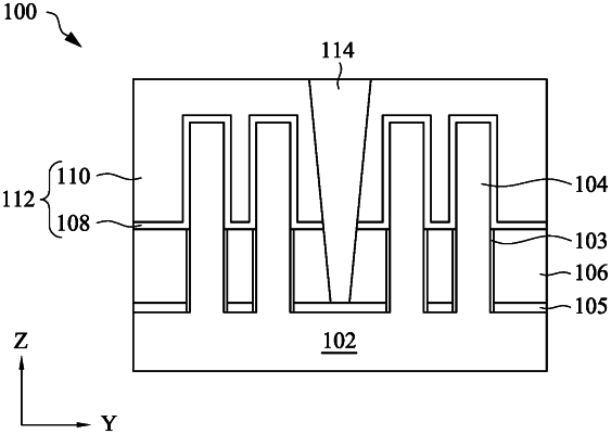
1. A device, comprising:
a substrate;
semiconductor fins extending from the substrate;
a liner layer on sidewalls of the semiconductor fins;
an etch stop layer over the substrate and extending laterally from a first portion of the liner layer on a first one of the semiconductor fins to a second portion of the line layer on a second one of the semiconductor fins;
an isolation structure over the etch stop layer, wherein the etch stop layer and the isolation structure include different materials;
a gate dielectric layer over a top surface of the isolation structure; and
a dielectric feature extending through the gate dielectric layer and into the isolation structure, wherein the isolation structure and the dielectric feature collectively extend laterally from the first portion of the liner layer to the second portion of the line layer.
|