| CPC H01L 21/823431 (2013.01) [H01L 21/823821 (2013.01); H01L 27/0886 (2013.01); H01L 27/0924 (2013.01)] | 20 Claims |

|
1. A method, comprising:
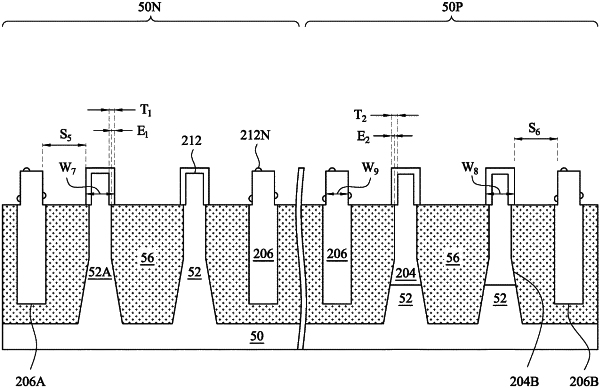
forming a first fin and a second fin within an insulation material over a substrate, the first fin and the second fin comprising different materials, the insulation material being interposed between the first fin and the second fin, the first fin having a first width and the second fin having a second width;
forming a first capping layer over the first fin;
forming a second capping layer over the second fin, the first capping layer having a first thickness, the second capping layer having a second thickness different from the first thickness; and
forming a first dielectric layer over the first capping layer and a second dielectric layer over the second capping layer, wherein forming the first dielectric layer comprises converting an entirety of the first capping layer to a first intermediate layer, and wherein forming the second dielectric layer comprises converting an upper portion of the second capping layer to a second intermediate layer with a lower portion of the second capping layer remaining unconverted.
|