| CPC H01L 21/823418 (2013.01) [H01L 21/823412 (2013.01); H01L 21/823431 (2013.01); H01L 21/823475 (2013.01); H01L 21/823481 (2013.01); H01L 23/535 (2013.01); H01L 27/0886 (2013.01); H01L 29/0653 (2013.01); H01L 29/0847 (2013.01); H01L 29/1037 (2013.01); H01L 29/66545 (2013.01); H01L 29/6681 (2013.01); H01L 29/161 (2013.01); H01L 29/165 (2013.01)] | 20 Claims |

|
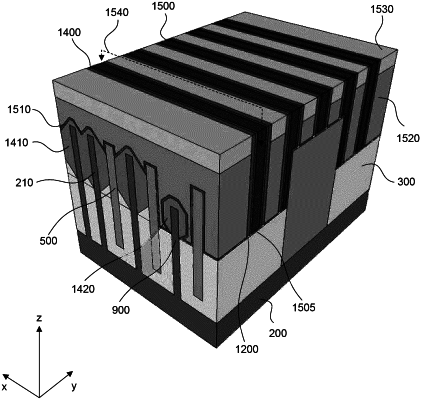
1. A structure, comprising:
a substrate;
a first semiconductor fin on the substrate;
a second semiconductor fin on the substrate, the second semiconductor fin being taller than the first semiconductor fin;
a first insulating fin over the substrate and between the first and the second semiconductor fins;
a second insulating fin on the substrate and adjacent to the first semiconductor fin, wherein the first semiconductor fin is positioned between the first and the second insulating fins;
a third insulating fin on the substrate and adjacent to the second semiconductor fin, wherein the second semiconductor fin is positioned between the first and the third insulating fins;
a first epitaxial stack on a portion of the first semiconductor fin; and
a second epitaxial stack on a portion of the second semiconductor fin, the second epitaxial stack being taller than the first epitaxial stack.
|