| CPC H01L 21/76245 (2013.01) [H01L 21/565 (2013.01); H01L 23/29 (2013.01); H01L 23/3121 (2013.01); H01L 23/3735 (2013.01); H01L 23/66 (2013.01); H01L 24/17 (2013.01)] | 10 Claims |

|
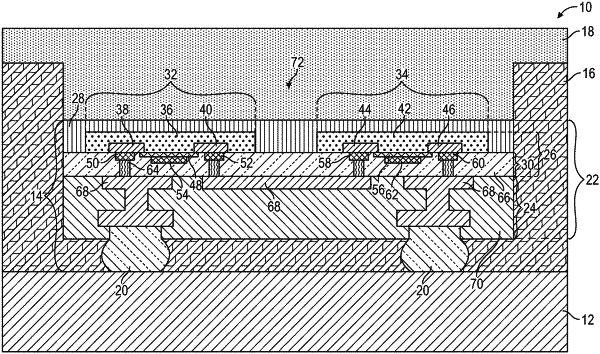
1. An apparatus comprising:
a device substrate having a top surface;
a thinned device die comprising a device region and a plurality of bump structures, wherein:
the device region comprises an isolation portion, a back-end-of-line (BEOL) portion with a plurality of connecting layers, and a front-end-of-line (FEOL) portion with a contact layer and a first active section;
the contact layer resides over the BEOL portion, the first active section resides over the contact layer, and the isolation portion resides over the contact layer and covers sides and a top surface of the first active section, such that a combination of the contact layer and the isolation portion fully encapsulates the first active section; and
the plurality of bump structures are formed at a bottom surface of the BEOL portion and attached to the top surface of the device substrate, wherein the plurality of bump structures are electrically coupled to the FEOL portion via certain ones of the plurality of connecting layers;
a first mold compound residing over the top surface of the device substrate, surrounding the thinned device die, and extending vertically beyond the thinned device die to define an opening over the thinned device die and within the first mold compound, wherein the first mold compound is not formed over the thinned device, and the isolation portion of the thinned device die is at the bottom of the opening; and
a second mold compound substantially filling the opening and in contact with the isolation portion.
|