| CPC H01L 21/67373 (2013.01) [H01L 21/67369 (2013.01); H01L 21/67386 (2013.01)] | 10 Claims |

|
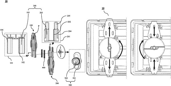
1. A latching guide structure which is arranged in a door of semiconductor carrier, wherein the latching guide structure comprises:
an upper latching part, having a first guiding portion, and the first guiding portion comprises an upper actuating unit;
a lower latching part, having a second guiding portion, and the second guiding portion comprises a lower actuating unit;
wherein the second guiding portion is configured to match a location of the first guiding portion, and the second guiding portion and the first guiding portion define an installation space;
at least one elastic unit, configured inside the installation space; and
a driver, engaged with the upper actuating unit and the lower actuating unit;
wherein the driver comprises a main driving portion and controlling portion which is connected with the main driving portion;
wherein the controlling portion is configured to control the main driving portion, the controlling portion simultaneously engages with the upper actuating unit and the lower actuating unit for linearly moving in reverse direction between the upper actuating unit and the lower actuating unit;
wherein the elastic unit represents a compression level or an extension level which are determined by linear movement between the upper actuating unit and the lower actuating unit, controlling the upper latching part and the lower latching part to be an open status or a close status.
|