| CPC H01L 21/4842 (2013.01) [H01L 21/565 (2013.01); H01L 23/3107 (2013.01); H01L 23/49503 (2013.01); H01L 23/49575 (2013.01)] | 23 Claims |

|
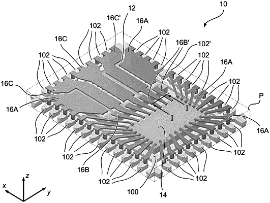
1. A method, comprising:
arranging a set of semiconductor dice on a die pad of a metallic leadframe, said set of semiconductor dice including a first semiconductor die and a second semiconductor die, wherein the first semiconductor die and the second semiconductor die each have sets of bonding pads at their front surfaces opposed to the die pad;
forming a layer of laser-activatable material on said first semiconductor die, said second semiconductor die, and a set of electrically-conductive leads of the metallic leadframe arranged around the die pad;
directing laser radiation on said layer of laser-activatable material to pattern a set of laser-activated lines, wherein said set of laser-activated lines include:
i) a first subset of laser-activated lines configured to couple selected bonding pads of one or more of said first semiconductor die and said second semiconductor die to selected electrically-conductive leads in said set of electrically-conductive leads;
ii) a second subset of laser-activated lines configured to couple selected bonding pads of said first semiconductor die to selected bonding pads of said second semiconductor die; and
iii) a third subset of laser-activated lines configured to couple each of said laser-activated lines in said second subset of laser-activated lines to one or more of at least one laser-activated line in said first subset of laser-activated lines, and at least one electrically-conductive lead in said set of electrically-conductive leads;
depositing a first metallic layer on said first, second, and third subsets of laser-activated lines to provide respective first, second, and third subsets of electrically-conductive lines;
selectively depositing a second metallic layer on said first and second subsets of electrically-conductive lines, but not the third subset of electrically-conductive lines, by electroplating to provide respective first and second subsets of electrically-conductive tracks; and
selectively removing said third subset of electrically-conductive lines.
|