| CPC H01L 21/30655 (2013.01) [H01L 21/02016 (2013.01); H01L 21/26506 (2013.01); H01L 21/3226 (2013.01); H01L 21/76 (2013.01); H01L 21/76264 (2013.01); H01L 23/3171 (2013.01); H01L 23/58 (2013.01); H01L 27/08 (2013.01); H01L 27/1203 (2013.01); H01L 29/0684 (2013.01); H01L 29/6634 (2013.01); H01L 23/291 (2013.01); H01L 29/0661 (2013.01)] | 14 Claims |

|
1. A device, comprising:
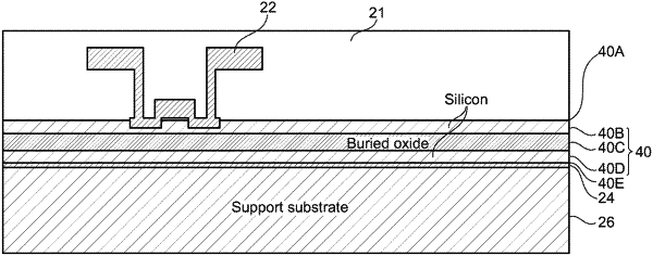
a semiconductor substrate having a first side and a second side opposite the first side, wherein a thickness of the semiconductor substrate is 70 μm or less;
at least one radio frequency device formed at the first side of the semiconductor substrate; and
a processed region at the second side of the semiconductor substrate, wherein the processed region is configured to provide additional ion gettering at the second side of the semiconductor substrate and wherein the processed region comprises one or more of:
an ion implanted layer;
a defect rich layer;
a doped layer with a dopant concentration higher than in a region adjacent to the doped layer;
an aluminum oxide layer; and
a reactive ion etched region,
wherein the at least one radio frequency device comprises at least two radio frequency devices, wherein the device further comprises:
at least one of an ion implanted region or an etched region from the second side of the semiconductor substrate limited to an area between the at least two radio frequency devices.
|