| CPC H01G 4/232 (2013.01) [H01G 2/065 (2013.01); H01G 4/30 (2013.01); H01G 4/1227 (2013.01)] | 11 Claims |

|
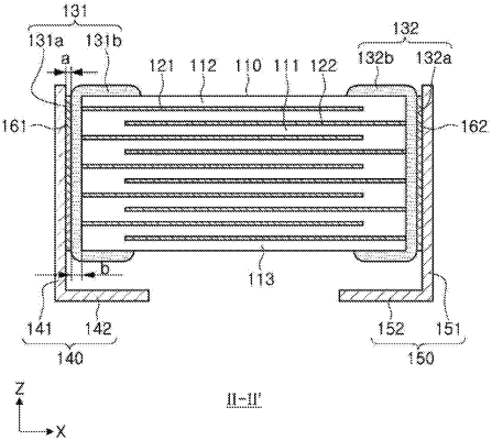
1. An electronic component comprising:
a body;
a pair of external electrodes, disposed on both ends of the body in a first direction, respectively, containing at least one of copper or nickel, while not containing a first noble metal;
a pair of metal frames connected to the pair of external electrodes, respectively; and
a pair of conductive bonding layers, disposed between the external electrodes and the pair of metal frames, respectively, containing a second noble metal,
wherein an entire length of at least one of the conductive bonding layers in a direction perpendicular to the first direction overlap the body along the first direction, and
wherein at least one of the external electrodes extend beyond both ends of the at least one of the conductive bonding layers in the direction perpendicular to the first direction.
|