| CPC G11C 16/3472 (2013.01) [G11C 16/08 (2013.01); G11C 16/14 (2013.01); G11C 16/24 (2013.01); G11C 16/26 (2013.01); G11C 16/30 (2013.01)] | 8 Claims |

|
1. A semiconductor memory apparatus comprising:
a memory cell array comprising a plurality of memory cells, wherein the memory cell array is a mini-array in a NOR flash memory, and the memory cells are configured to store option bits or status bits;
a switch circuit coupled to the memory cell array and comprising at least one switch, wherein each of the at least one switch receives a control signal, and is turned on or off under control of the control signal; and
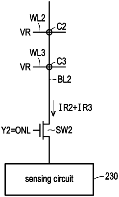
a sensing circuit coupled to the switch circuit, wherein when an erase verification is performed, the sensing circuit sequentially receives an erase verification current generated by each of the memory cells through the switch circuit to verify an erase state of the each of the memory cells,
wherein when a read operation is performed by applying a reading voltage to the memory cell array during power-up, the sensing circuit simultaneously receives a reading current generated by the each of the memory cells through the switch circuit and compares a summed current resulting from summing of the reading currents with a reference current,
wherein the reading voltage during power-up is less than the erase verification voltage used for verifying the erase state.
|