| CPC G11C 13/0038 (2013.01) [G11C 13/0026 (2013.01); G11C 13/003 (2013.01)] | 20 Claims |

|
1. A memory device, comprising:
a memory array including a plurality of memory cells arranged in rows and columns;
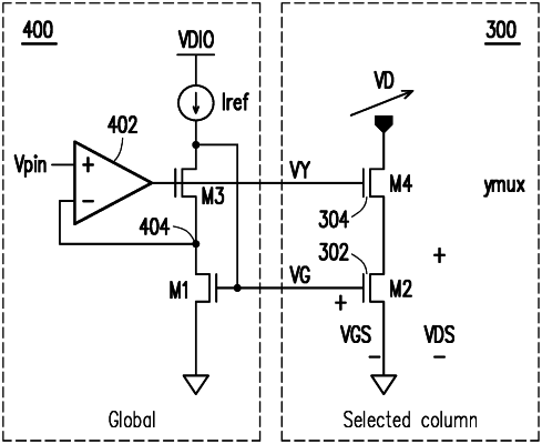
a current limiter coupled to a plurality of the columns of the memory array and comprising a cascode of first and second connected NMOS transistors;
a closed loop bias generator comprising third and fourth cascode connected NMOS transistors, the closed loop bias generator configured to output a column select signal to the memory array that is received by the current limiter; and
an operational amplifier configured to receive a feedback signal and generate a column select signal output to a column MUX, wherein the output of the operational amplifier is connected to a gate of the first NMOS transistor, and a source of the third NMOS transistor is connected to a gate of the second NMOS transistor.
|