| CPC G11C 11/419 (2013.01) [G11C 5/147 (2013.01); G11C 7/12 (2013.01); G11C 11/412 (2013.01); G11C 11/418 (2013.01); H03K 19/0136 (2013.01)] | 20 Claims |

|
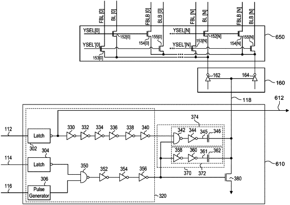
1. A circuit, comprising:
a first capacitive element;
a second capacitive element; and
a logic circuit configured to:
receive row address information associated with first memory cells in a first portion of a memory region and with second memory cells in a second portion of the memory region; and
control a reference voltage provided to first bitlines coupled to the first memory cells in the first portion of the memory region and second bitlines coupled to the second memory cells coupled to the second memory cells in the second portion of the memory region,
wherein the second bitlines are longer than the first bitlines,
wherein, in response to the row address information being associated with at least one of the first memory cells, the logic circuit is configured to couple, via the first capacitive element, the reference voltage to a first negative voltage applied to the first bitlines coupled to the first memory cells in the first portion of the memory region,
wherein, in response to the row address information being associated with at least one of the second memory cells, the logic circuit is configured to couple, via the first and second capacitive elements, the reference voltage to a second negative voltage lower than the first negative voltage, and
wherein the second negative voltage is applied to the second bitlines coupled to the second memory cells in the second portion of the memory region.
|