| CPC G09G 3/3266 (2013.01) [G11C 19/28 (2013.01); G09G 2300/0426 (2013.01); G09G 2300/0852 (2013.01); G09G 2310/0286 (2013.01); G09G 2310/0294 (2013.01); G09G 2330/021 (2013.01)] | 18 Claims |
|
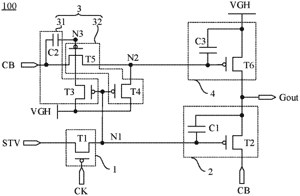
1. A shift register, comprising:
an input circuit electrically connected to a first clock signal terminal, an input signal terminal and a first node, the input circuit being configured to transmit an input signal received at the input signal terminal to the first node under control of a first clock signal transmitted by the first clock signal terminal;
an output circuit electrically connected to the first node, a second clock signal terminal and an output signal terminal, the output circuit being configured to transmit a second clock signal received at the second clock signal terminal to the output signal terminal under control of a voltage of the first node;
a first control circuit electrically connected to the first node, a first voltage signal terminal, the second clock signal terminal and a second node, the first control circuit being configured to, according to one of a first voltage signal transmitted by the first voltage signal terminal and the second clock signal, control a voltage of the second node under control of the voltage of the first node and the second clock signal; and
a holding circuit electrically connected to the second node, the first voltage signal terminal and the output signal terminal, the holding circuit being configured to transmit the first voltage signal to the output signal terminal under control of the voltage of the second node,
wherein the first control circuit includes a first control sub-circuit and a second control sub-circuit,
wherein the first control sub-circuit is electrically connected to the first node, the first voltage signal terminal, the second clock signal terminal and a third node; the first control sub-circuit is configured to, according to one of the first voltage signal and the second clock signal, control a voltage of the third node under the control of the voltage of the first node and the second clock signal; and
the second control sub-circuit is electrically connected to the first node, the third node, the first voltage signal terminal, the second clock signal terminal and the second node the second control sub-circuit is configured to, according to one of the first voltage signal and the second clock signal, control the voltage of the second node under control of the voltage of the first node and the voltage of the third node,
wherein the first control sub-circuit includes a third transistor and a second capacitor,
wherein a control electrode of the third transistor is electrically connected to the first node, a first electrode of the third transistor is electrically connected to the first voltage signal terminal, and a second electrode of the third transistor is electrically connected to the third node; and
a first end of the second capacitor is electrically connected to the second clock signal terminal, and a second end of the second capacitor is electrically connected to the third node,
wherein the output circuit includes a second transistor and a first capacitor, wherein a control electrode of the second transistor is electrically connected to the first node, a first electrode of the second transistor is electrically connected to the second clock signal terminal, and a second electrode of the second transistor is electrically connected to the output signal terminal; and
a first end of the first capacitor is electrically connected to the first node, and a second end of the first capacitor is electrically connected to the output signal terminal.
|