| CPC G09G 3/2092 (2013.01) [G09G 2300/0426 (2013.01); G09G 2354/00 (2013.01)] | 18 Claims |

|
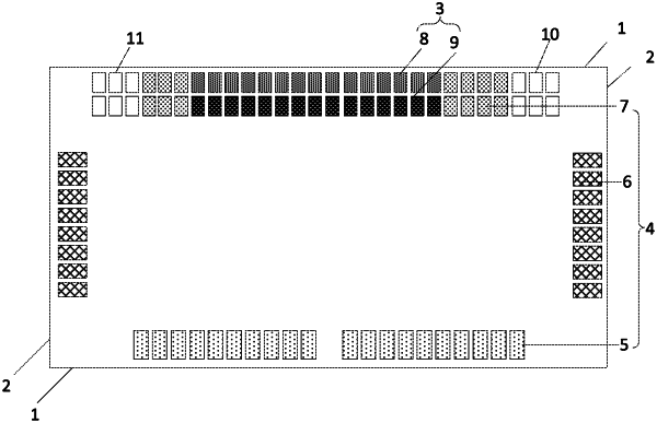
1. A driver chip, comprising: two opposite long edges, and two opposite short edges connected to the long edges, wherein the driver chip comprises: a plurality of output pins and a plurality of input pins;
the plurality of output pins are close to one of the long edges;
the plurality of input pins comprises: first input pins, second input pins and third input pins;
the first input pins are close to the other long edge opposite to the plurality of output pins;
the second input pins are close to the short edges; and
the third input pins are close to one of the long edges and arranged on both sides of the plurality of output pins;
wherein the driver further comprises: a plurality of gate drive signal input pins, and a plurality of gate drive signal output pins electrically connected to the gate drive signal input pins in a one-to-one corresponding mode;
wherein the gate drive signal input pins and the gate drive signal output pins are close to one of the long edges and arranged on both sides of the third input pins, respectively.
|