| CPC G06F 9/44505 (2013.01) [G06F 1/24 (2013.01); G06F 1/26 (2013.01); G06F 13/4282 (2013.01); G06F 21/572 (2013.01); G06F 21/575 (2013.01); G06F 21/81 (2013.01); G06F 2213/0016 (2013.01); G06F 2221/034 (2013.01)] | 10 Claims |
|
1. A non-transitory machine-readable storage media having machine-readable instructions stored thereon, that when executed, cause one or more machines, to perform a method comprising:
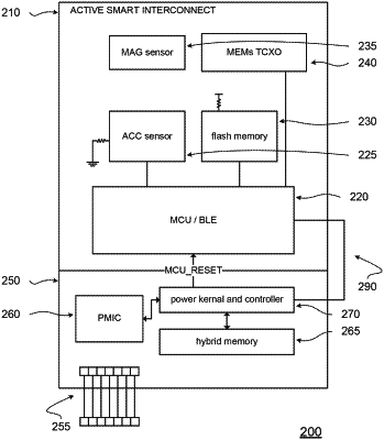
placing a semiconductor interconnect substrate into a power-up mode, the semiconductor interconnect substrate being electrically coupled to one or more components mounted thereon; and
applying a configuration command set to the one or more components in a normal operation mode subsequent to the power-up mode, wherein applying the configuration command set comprises sequencing configuration of the one or more components based on configuration register values associated with a boot configuration, wherein the configuration command set encompasses a resistor disconnection command that establishes a strapping or logical value on an interface of a component, of the one or more components, with a plurality of strapping pins coupled to the component, and wherein the plurality of strapping pins are operable to configure a static behavior of an interconnect of the semiconductor interconnect substrate.
|