| CPC G06F 30/398 (2020.01) [G06N 3/04 (2013.01); G06N 3/063 (2013.01); G06N 3/08 (2013.01); H01L 22/12 (2013.01); G06F 2119/22 (2020.01)] | 20 Claims |

|
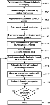
1. A method, comprising:
preparing a first plurality of samples of an integrated circuit for imaging;
generating electron microscope images of the first plurality of prepared samples of the integrated circuit;
training a neural network to generate pixel level masks of features of the first plurality of the samples of the integrated circuit from the electron microscope images, comprising:
generating pixel level feature maps of the first plurality of the samples of the integrated circuit from the electron microscope images;
generating bounding box predictions from the pixel level feature maps;
introducing added error into the bounding box predictions;
locating regions of interest within the pixel level feature maps; and
generating the pixel level masks of features of the first plurality of the samples of the integrated circuits for the located regions of interest from the bounding box predictions with the introduced added error;
applying the trained neural network to one or more additional samples of the integrated circuit to generate pixel level masks of features of the one or more additional samples of the integrated circuit from the bounding box predictions with the introduced added error;
analyzing results of the application of the trained neural network to the one or more additional samples of the integrated circuit;
adjusting processing for fabrication of the integrated circuit based upon the analyzing of the results of the application of the trained neural network to the one or more additional samples of the integrated circuit; and
fabricating the integrated circuit by the adjusted processing.
|