| CPC G06F 30/333 (2020.01) [G06F 30/327 (2020.01); G01R 31/318583 (2013.01)] | 20 Claims |

|
1. A system comprising:
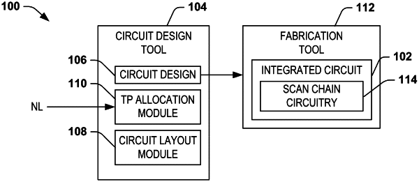
a non-transitory memory that stores machine-readable instructions and receives a circuit netlist associated with a circuit design, the circuit netlist comprising functional logic, test-point nodes interconnecting portions of the functional logic, and a plurality of test-point flops associated with scan-chains; and
a processing unit that accesses the memory and executes the machine-readable instructions, the machine-readable instructions comprising an electronic design automation (EDA) application, the EDA application comprising:
a test-point flop allocation module that is configured to evaluate the circuit netlist to determine compatibility of the test-point nodes in the circuit netlist, the test-point flop allocation module being further configured to allocate each of the test-point flops to one of a plurality of test-point sharing groups comprising a plurality of compatible test-point nodes; and
a circuit layout module configured to generate a circuit layout associated with the circuit design, the circuit layout comprising the functional logic and scan-chains comprising the test-point flops allocated to the test-point sharing groups in response to the circuit netlist.
|