| CPC G06F 3/0629 (2013.01) [G06F 3/0679 (2013.01); G06F 13/1668 (2013.01); G11C 7/10 (2013.01)] | 29 Claims |

|
1. A memory device, comprising:
a memory die that comprises an input/output (I/O) pad operable to couple with a host device;
an input buffer included in the memory die, the input buffer coupled with the I/O pad;
a capacitive component having an adjustable capacitance and included in the memory die, the capacitive component coupled with the I/O pad;
one or more mode registers; and
circuitry operable to cause the memory device to:
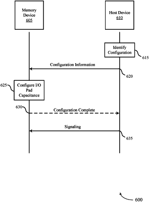
receive an indication from the host device to store configuration information associated with the adjustable capacitance of the capacitive component to the one or more mode registers;
store the configuration information to the one or more mode registers;
configure the adjustable capacitance of the capacitive component based at least in part on the configuration information stored in the one or more mode registers; and
receive signaling from the host device via the I/O pad based at least in part on configuring the capacitive component.
|