| CPC G06F 3/0619 (2013.01) [G06F 3/0655 (2013.01); G06F 3/0656 (2013.01); G06F 3/0679 (2013.01)] | 20 Claims |

|
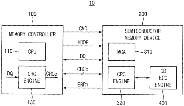
1. A semiconductor memory device comprising:
a memory cell array comprising a plurality of volatile memory cells coupled to respective ones of a plurality of word-lines and respective ones of a plurality of bit-lines; and
a cyclic redundancy check (CRC) engine configured to perform, during a memory operation on the memory cell array, operations comprising:
detecting an error in a main data and a system parity data received from a memory controller through a link, wherein the memory controller is external to the semiconductor memory device;
generating an error flag indicating whether the error that was detected corresponds to either a first type of error associated with the link or a second type of error associated with the volatile memory cells based on the system parity data; and
transmitting the error flag to the memory controller.
|