| CPC G06F 3/047 (2013.01) [G06F 3/044 (2013.01); G06F 3/04146 (2019.05); G06F 2203/04112 (2013.01)] | 9 Claims |

|
1. A touch sensor comprising:
a substrate including a sensing area and a non-sensing area;
a first touch electrode disposed on the sensing area of the substrate;
a pad part disposed on the non-sensing area of the substrate;
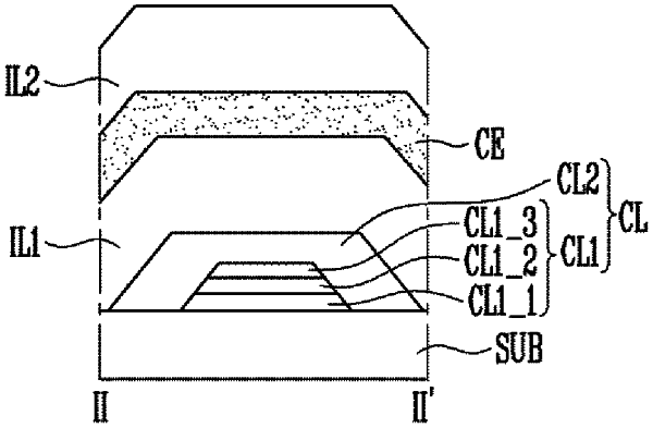
a connection line disposed entirely in the non-sensing area and electrically connecting the first touch electrode and the pad part, the connection line including a first connection line and a second connection line surrounding upper and side surfaces of the first connection line;
a first insulating layer disposed on the connection line in the non-sensing area, the first insulating layer including a first contact hole disposed in the non-sensing area and exposing a portion of the second connection line;
a connection electrode formed on the first insulating layer and comprising a first portion extending to the non-sensing area in a first direction from one end of the first touch electrode, a second portion extending from the first portion of the connection electrode in a second direction intersecting the first direction, and a third portion extending from the second portion of the connection electrode in the second direction, wherein the second portion has a first width in the first direction, the third portion has a second width in the first direction, the first width is greater than the second width, and the first portion of the connection electrode physically contacts the exposed portion of the second connection line through the first contact hole in the first insulating layer; and
a second touch electrode disposed on the sensing area of the substrate and spaced apart from the first touch electrode in the second direction,
wherein:
the second portion of the connection electrode faces one end of the first touch electrode in the first direction;
the connection electrode and the connection line overlap each other for an entire length of the connection line to extend to the pad part in the non-sensing area, the third portion of the connection electrode is spaced apart from the connection line with the first insulating layer interposed therebetween;
the connection electrode is disposed on the first insulating layer, which is in the non-sensing area, and extends to the pad part; and
the first connection line has a triple layer structure comprising stacked layers of molybdenum (Mo), aluminum (Al), and molybdenum (Mo) having thicknesses of 200 Å, 3000 Å, and 500 Å, respectively.
|