US 11,947,479 B2
Dynamic timing calibration systems and methods
Jens Kristian Poulsen, Kitchener (CA)
Assigned to Google LLC, Mountain View, CA (US)
Filed by Google LLC, Mountain View, CA (US)
Filed on Apr. 26, 2023, as Appl. No. 18/139,688.
Application 18/139,688 is a continuation of application No. 17/068,766, filed on Oct. 12, 2020, granted, now 11,657,010.
Application 17/068,766 is a continuation in part of application No. 16/455,625, filed on Jun. 27, 2019, granted, now 11,294,837.
Claims priority of provisional application 62/914,351, filed on Oct. 11, 2019.
Claims priority of provisional application 62/853,654, filed on May 28, 2019.
Claims priority of provisional application 62/824,985, filed on Mar. 27, 2019.
Claims priority of provisional application 62/791,607, filed on Jan. 11, 2019.
Claims priority of provisional application 62/721,412, filed on Aug. 22, 2018.
Prior Publication US 2023/0259473 A1, Aug. 17, 2023
Int. Cl. G06F 13/362 (2006.01); G06F 1/12 (2006.01); G06F 13/40 (2006.01); G06F 13/42 (2006.01); H04L 7/00 (2006.01)
CPC G06F 13/3625 (2013.01) [G06F 1/12 (2013.01); G06F 13/4004 (2013.01); G06F 13/423 (2013.01); H04L 7/0037 (2013.01)] 20 Claims
OG exemplary drawing
 
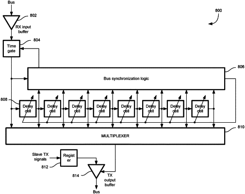
1. An internal delay correction circuit, comprising:
an input connected with a line of a bus, wherein the line of the bus is used for time-multiplexed clock and data communication;
a time-gate that filters data traffic on the line of the bus from synchronization pulses;
a plurality of delay cells;
a bus synchronization circuit that controls the plurality of delay cells;
a multiplexer that is used to control output timing using the plurality of delay cells; and
an output connected with the line of the bus, wherein the output timing controlled by the multiplexer controls timing of data output via the output.