| CPC G03F 7/38 (2013.01) [G03F 7/0042 (2013.01)] | 20 Claims |
|
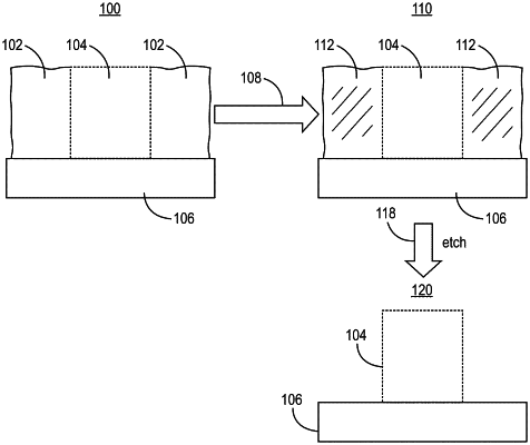
1. A method for forming a radiation patternable organo tin-based coating on a wafer, the coating having an average thickness from about 1 nm to about 500 nm, the method comprising:
contacting the wafer with the coating with an atmosphere comprising a CO2 concentration from about 0.1 mole percent to about 10 mole percent prior to development to form a physical pattern having an increased critical dimension for a given exposure dose relative to a corresponding wafer not contacted with the atmosphere with CO2, the coating comprising a composition represented by the formula RSnOxOH3-x wherein R is an organic ligand with 1-31 carbon atoms, with a carbon atom bonded to Sn and with one or more carbon atoms optionally substituted with one or more heteroatom functional groups, wherein the remaining atmosphere comprises an inert gas.
|