| CPC G02F 1/1339 (2013.01) [G02F 1/134309 (2013.01); H05K 1/0296 (2013.01); H05K 1/14 (2013.01); G02F 1/134372 (2021.01); G02F 1/13439 (2013.01)] | 13 Claims |

|
1. An electronic device, comprising:
a first substrate comprising a peripheral area;
a first inorganic insulating layer disposed on the first substrate;
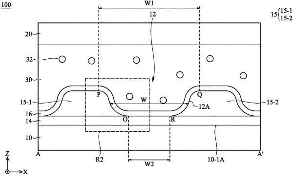
an insulating layer disposed on the first inorganic insulating layer and formed a recess and another recess adjacent to the recess, wherein the recess and the another recess are disposed in the peripheral area; and
a second inorganic insulating layer disposed on the insulating layer and formed in the recess,
wherein a thickness of the second inorganic insulating layer is less than a thickness of the insulating layer,
wherein the recess has a top portion and a bottom portion, and the bottom portion is between the top portion and the first substrate, the top portion has a first width, the bottom portion has a second width, and the first width is greater than the second width,
wherein in a top view, the recess extends in a first direction parallel to an edge of the first substrate, and a maximum width of the recess is greater than a gap between the recess and the another recess in the first direction parallel to the edge of the first substrate.
|