| CPC G02F 1/035 (2013.01) [G02B 6/12004 (2013.01); G02F 1/0147 (2013.01); G02F 2201/063 (2013.01)] | 20 Claims |

|
1. A manufacturing method, comprising:
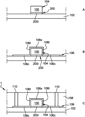
forming a waveguide from a first material, the waveguide used to guide an optical signal, the waveguide having a first side adjacent to an insulating layer, a second side and a third side perpendicular to the first side, and a fourth side parallel to the first side; and
forming a layer made of a second material, the second material being electrically conductive and transparent to a wavelength of the optical signal, the layer being disposed over the first side, the second side, the third side, and the fourth side of the waveguide, the layer being in direct contact with the first side, the second side, the third side, the fourth side, or a combination thereof.
|