| CPC G02B 6/305 (2013.01) [G02B 6/12004 (2013.01); G02B 6/1228 (2013.01); G02B 2006/12147 (2013.01); G02B 2006/12166 (2013.01)] | 19 Claims |
|
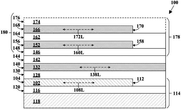
1. A stacked edge coupler, comprising:
an insulator layer;
a first assisting waveguide on the insulator layer, the first assisting waveguide comprises an end surface;
a waveguide core over the first assisting waveguide, the waveguide core comprising a tapered section having an end surface, and the end surface of the tapered section of the waveguide core is substantially coplanar with the end surface of the first assisting waveguide; and
a back-end-of-line stack over the waveguide core, the back-end-of-line stack comprises:
a side edge;
a dielectric layer; and
a second assisting waveguide on the dielectric layer adjacent to the side edge, and the second assisting waveguide has an overlapping arrangement with the tapered section of the waveguide core.
|