| CPC G01R 1/071 (2013.01) [G01R 1/073 (2013.01); G01R 31/311 (2013.01); G02B 6/26 (2013.01); G02B 26/0816 (2013.01)] | 25 Claims |

|
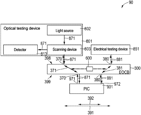
1. A system, comprising:
an electro-optical circuit board, comprising:
an electrical conductor track extending between first and second sides of the electro-optical circuit board; and
an optical beam path extending between the first and second sides of the electro-optical circuit board; and
an optical testing device, comprising:
a light source; and
a scanning device,
wherein:
the optical testing device is configured to drive the light source and the scanning device so that when the optical testing device drives the light source and the scanning device: i) the light source emits a light beam; and ii) the scanning device varies a location of the light beam on a first side of the electro-optical circuit board;
the electrical conductor track is configured to contact an electrical interface of a photonic integrated circuit adjacent the second side of the electrical conductor track; and
the optical beam path is configured to contact an optical interface of the photonic integrated circuit adjacent the second side of the electrical conductor track.
|