| CPC B81B 3/0051 (2013.01) [B81C 1/00595 (2013.01); B81B 2201/0235 (2013.01); B81B 2201/0242 (2013.01); B81C 2201/0198 (2013.01)] | 16 Claims |
|
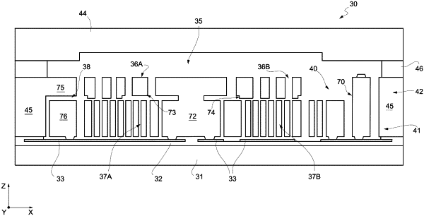
1. A MEMS device, comprising:
a substrate;
a first structural layer having a first thickness and extending on the substrate;
a second structural layer having a second thickness and extending on the first structural layer;
a plurality of first trenches extending through the first structural layer and defining first functional elements;
a plurality of second trenches extending through the second structural layer and defining second functional elements overlying the first functional elements; and
a plurality of third trenches extending through the first and the second structural layers,
wherein the first and the second structural layers form a supporting structure, the supporting structure having a third thickness equal to the sum of the first and the second thicknesses, and the supporting structure being anchored to the substrate and supporting the first and the second functional elements,
wherein one or more respective third trenches of the plurality of third trenches have the third thickness, and
wherein a first gap zone extends between the first and the second functional elements and surrounds the supporting structure.
|