| CPC A61B 1/0607 (2013.01) [A61B 1/00096 (2013.01); A61B 1/00135 (2013.01); A61B 1/043 (2013.01); A61B 1/05 (2013.01); H01L 25/167 (2013.01); H04N 23/54 (2023.01); H04N 25/53 (2023.01); H04N 25/76 (2023.01); A61B 1/0051 (2013.01); A61B 1/07 (2013.01); H01L 2924/0002 (2013.01); H01L 2924/3011 (2013.01); H04N 23/555 (2023.01)] |

| AS A RESULT OF REEXAMINATION, IT HAS BEEN DETERMINED THAT: |
| Claims 1, 2 and 13 are cancelled. |
| Claims 3-12, 14 and 15 were not reexamined. |
|
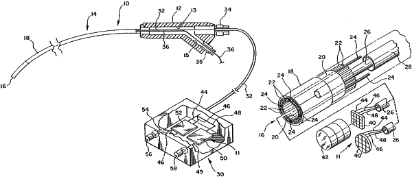
an image sensor lying in a first plane and including an array of pixels for receiving images thereon, said image sensor further including circuitry means on said first plane and coupled to said array of pixels for timing and control of said array of pixels, said image sensor producing a pre-video signal;
a first circuit board lying in a second plane and communicating with said image sensor by at least one pre-video conductor inner-connecting said image sensor and said first circuit board, said first circuit board including circuitry means for converting said pre-video signal to a post-video signal for reception by a standard video device;
a power supply coupled with said image sensor for driving said array of pixels and said timing and control means, and electrically coupled to said first circuit board for driving said first circuit board; and
a time select switch electrically communicating with said first circuit board and remote from said first circuit board for selectively varying integration periods to produce an image of a desired brightness, said switch having a plurality of settings enabling selective control to produce the image of a desired brightness.
|