|
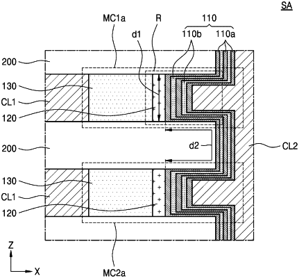
1. A semiconductor apparatus comprising: a substrate; a first insulating layer and a second insulating layer that are apart from each other in a direction normal to the substrate; and a semiconductor unit device between the first insulating layer and the second insulating layer, wherein the semiconductor unit device includes a selection device layer and a phase change material layer that extend side by side in a direction parallel to the substrate, the phase change material layer includes a first chalcogen layer including GexTe1-x (0.3≤x≤0.7) and a second chalcogen layer including SbyTe1-y (0.2≤y≤0.8), the selection device layer forms a recess portion by covering a portion of a surface of the first insulating layer and a portion of a surface of the second insulating layer such that a sidewall of the selection device layer is recessed relative to a sidewall of the first insulating layer and a sidewall of the second insulating layer, the phase change material layer is arranged along the recess portion to cover the first insulating layer, the selection device layer, and the second insulating layer, and a length of a surface of the phase change material layer adjacent to the first insulating layer is equal to or greater than a length of a surface of the phase change material layer adjacent to the selection device layer, wherein, the length of the surface of the phase change material layer adjacent to the first insulating layer is greater than the length of the surface of the phase change material layer adjacent to the selection device layer by a factor of greater than about 1.0 to about 5.0, a first portion of the phase change material layer extends in a first direction along the first insulating layer, a second portion of the phase change material layer extends in the first direction along the second insulating layer, a third portion of the phase change material extends in a second direction and connects the first portion of the phase change material layer to the second portion of the phase change material layer, the first direction and second direction intersect each other, and the first portion of the phase change material layer and the second portion of the phase change material layer are spaced apart from each other in the second direction and extend in the first direction from opposite ends of the third portion of the phase change material layer a surface of the first portion of the phase change material layer is spaced apart in the second direction from a surface of the second portion of the phase change material layer.
|