| CPC H10N 50/10 (2023.02) [H01L 23/5283 (2013.01); H10B 61/22 (2023.02); H10N 50/01 (2023.02); H10N 50/80 (2023.02)] | 20 Claims |
|
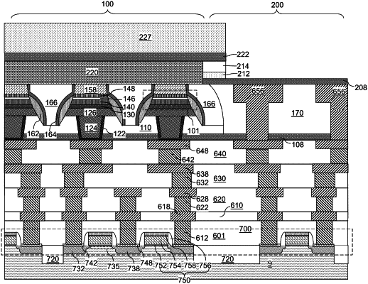
1. A method of manufacturing a memory array device, comprising;
forming an array of memory cells over a substrate by depositing and patterning a memory material layer stack, wherein each of the memory cells comprises, from bottom to top, a bottom electrode, a memory element, and a top electrode;
forming a memory-level dielectric layer around the array of memory cells;
planarizing the top electrodes of the array of memory cells by removing portions of the top electrodes from above a horizontal plane located above bottom surfaces of the top electrodes; and
forming top-interconnection metal lines by depositing and patterning a conductive material above the memory-level dielectric layer, wherein the top-interconnection metal lines are formed on, or replaces, a respective row of top electrodes within the memory cells.
|