US 12,268,096 B2
Spacer stack for magnetic tunnel junctions
Joung-Wei Liou, Hsinchu (TW); and Chin Kun Lan, Hsinchu (TW)
Assigned to Taiwan Semiconductor Manufacturing Co., Ltd., Hsinchu (TW)
Filed by Taiwan Semiconductor Manufacturing Co., Ltd., Hsinchu (TW)
Filed on Jul. 31, 2023, as Appl. No. 18/228,282.
Application 17/135,637 is a division of application No. 16/129,088, filed on Sep. 12, 2018, granted, now 10,879,456, issued on Dec. 29, 2020.
Application 18/228,282 is a continuation of application No. 17/135,637, filed on Dec. 28, 2020, granted, now 11,785,858.
Claims priority of provisional application 62/690,724, filed on Jun. 27, 2018.
Prior Publication US 2023/0413680 A1, Dec. 21, 2023
Int. Cl. H10N 50/10 (2023.01); H10B 61/00 (2023.01); H10N 50/01 (2023.01); H10N 50/80 (2023.01); H10N 50/85 (2023.01)
CPC H10N 50/10 (2023.02) [H10B 61/20 (2023.02); H10N 50/01 (2023.02); H10N 50/80 (2023.02); H10N 50/85 (2023.02)] 20 Claims
OG exemplary drawing
 
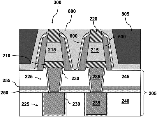
11. A semiconductor device, comprising:
an interconnect layer comprising a first dielectric layer and a conductive structure;
first and second magnetic tunnel junction (MTJ) structures disposed on the interconnect layer, wherein the first and second MTJ structures comprise first and second sidewalls, respectively, facing each other; and
a spacer stack disposed between the first and second MTJ structures, wherein the spacer stack comprises:
first and second nitride layers disposed on the first and second sidewalls, respectively;
a continuous metal-based layer disposed on the first and second nitride layers; and
a second dielectric layer disposed on the continuous metal-based layer.