| CPC H10K 59/131 (2023.02) [H10K 50/80 (2023.02); H10K 59/126 (2023.02); H10K 2102/311 (2023.02)] | 15 Claims |
|
1. A displaying substrate for preventing short circuit between auxiliary electrodes, wherein the auxiliary electrodes comprise a first auxiliary electrode and a second auxiliary electrode for reducing voltage drop of trace, and the displaying substrate comprises:
a flexible base plate;
a first metal layer arranged on one side of the flexible base plate and comprising the first auxiliary electrode, wherein the first auxiliary electrode is directly connected with a first power cord, the first auxiliary electrode is arranged on a same layer as the first power cord, the first auxiliary electrode is to ensure uniformity of voltage applied by the first power cord, and the first power cord is one of a VDD signal wire and a VSS signal wire; and
a pixel unit arranged on a side of the flexible base plate away from the first metal layer, the pixel unit comprising:
a plurality of thin-film transistors arranged on the side of the flexible base plate away from the first metal layer, and
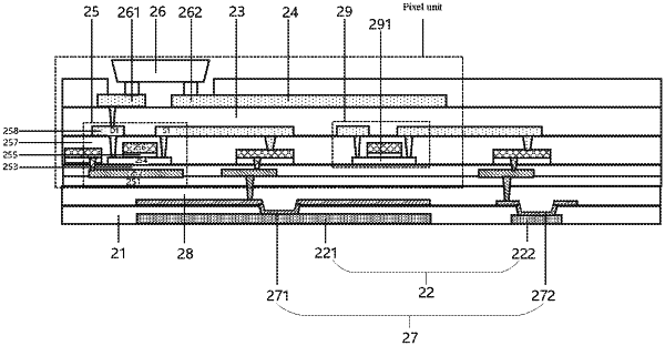
an insulation layer and the second auxiliary electrode arranged in layer configuration on a side of the plurality of thin-film transistors away from the flexible base plate, wherein the insulation layer is arranged between the second auxiliary electrode and the flexible base plate, the second auxiliary electrode is directly connected with a second power cord, the second auxiliary electrode is arranged on a same layer as the second power cord, the second auxiliary electrode is to ensure uniformity of voltage applied by the second power cord, and the second power cord is the other one of the VDD signal wire and the VSS signal wire;
wherein the plurality of thin-film transistors comprise a drive transistor, a source of the drive transistor is connected with the first auxiliary electrode, a drain of the drive transistor is connected with a first electrode of a light emitting device, and a second electrode of the light emitting device is connected with the second auxiliary electrode;
wherein the displaying substrate further comprises a second metal layer and a flat layer, wherein the second metal layer and the flat layer are arranged in layer configuration between the flexible base plate and the pixel unit, the second metal layer is arranged between the flat layer and the flexible base plate, the second metal layer comprises a jumper electrode, the jumper electrode is connected with the first auxiliary electrode through a via hole formed in the flexible base plate, and the jumper electrode is further connected with the source of the drive transistor;
wherein the drive transistor comprises a barrier layer, a light shielding layer, a buffer layer, an active layer, a grid insulating layer, a grid electrode, an interlayer dielectric layer and a source-drain electrode that are arranged in layer configuration on one side of the flat layer away from the flexible base plate; and
wherein the barrier layer is arranged between the light shielding layer and the flexible base plate, the insulating layer is arranged on a side of a source-drain electrode away from the flexible base plate, the source-drain electrode comprises the source and the drain of the drive transistor, and the source of the drive transistor is connected with the jumper electrode through via holes formed in the interlayer dielectric layer, the grid insulating layer, the buffer layer, the barrier layer and the flat layer.
|