| CPC H10K 59/1213 (2023.02) [H10K 71/00 (2023.02); H10D 30/0314 (2025.01); H10D 30/0321 (2025.01); H10D 30/6731 (2025.01); H10D 30/6745 (2025.01); H10D 86/0223 (2025.01); H10D 86/0231 (2025.01); H10D 86/421 (2025.01); H10D 86/60 (2025.01); H10K 59/1201 (2023.02)] | 19 Claims |
|
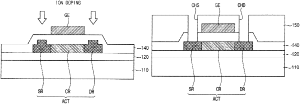
1. A method of manufacturing a display device, the method comprising:
forming a polysilicon layer on a substrate;
patterning the polysilicon layer to form a polysilicon pattern including a first region and a second region each having a first thickness, and a third region having a second thickness less than the first thickness;
forming a gate insulation layer on the polysilicon pattern;
forming a gate electrode on the gate insulation layer;
implanting ions into part of the polysilicon pattern to form an active layer, after forming the gate electrode;
forming an insulation interlayer on the gate electrode;
forming a source contact hole and a drain contact hole, each of the source contact hole and the drain contact hole passing through the insulation interlayer and the gate insulation layer and respectively overlapping the first region and the second region;
forming a source electrode and a drain electrode respectively filling the source contact hole and the drain contact hole; and
forming a light emitting element electrically connected to the source electrode or the drain electrode,
wherein forming the source contact hole and the drain contact hole includes flattening an upper surface of the active layer.
|